- 您现在的位置:买卖IC网 > Sheet目录307 > ADE7761BARSZ-RL (Analog Devices Inc)IC ENERGY METERING 1PHASE 20SSOP
�� �
�
�ADE7761B�
�=� 0� .� 367� Hz�
�F� 1� 2� Frequency� =�
�2� � 2� � 2� .� 5� 2�
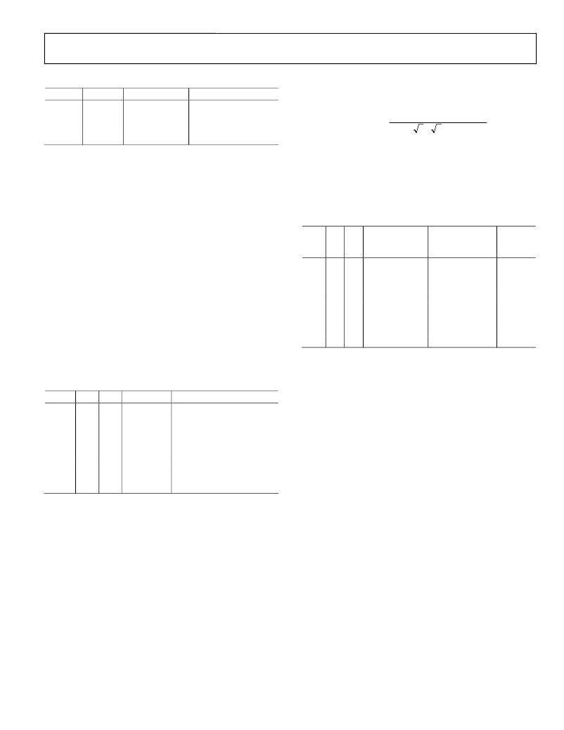
�Table� 6.� f� 1–4� Frequency� Selection�
�S1� S0� f� 1–4� (Hz)� 1�
�0� 0� 1.72�
�0� 1� 3.44�
�1� 0� 6.86�
�f� 1?4� =� OSC/2� n2�
�OSC/2� 18�
�OSC/2� 17�
�OSC/2� 16�
�Note� that� if� the� on-chip� reference� is� used,� actual� output�
�frequencies� may� vary� from� device� to� device� due� to� a� reference�
�tolerance� of� ±8%.�
�6� .� 13� � 0� .� 66� � 0� .� 66� � 1� .� 72� Hz�
�,� F�
�1�
�1�
�13.7�
�OSC/2� 15�
�CF� Frequency� =� F� 1� ,� F� 2� � 64� =� 23.5� Hz�
�Values� are� generated� using� the� nominal� frequency� of� 450� kHz.�
�f� 1–4� are� a� binary� fraction� of� the� master� clock� and,� therefore,� vary� with� the�
�1�
�2�
�internal� oscillator� frequency� (OSC).�
�Frequency� Output� CF�
�The� pulse� output� calibration� frequency� (CF)� is� intended� for� use�
�during� calibration.� The� output� pulse� rate� on� CF� can� be� up� to�
�2048� times� the� pulse� rate� on� F1� and� F2.� The� lower� the� f� 1–4�
�As� can� be� seen� from� these� two� example� calculations,� the� maximum�
�output� frequency� for� ac� inputs� is� always� half� of� that� for� dc� input�
�signals.� Table� 8� shows� a� complete� listing� of� all� maximum� output�
�frequencies� for� ac� signals.�
�Table� 8.� Maximum� Output� Frequencies� on� CF,� F1,� and� F2� for�
�AC� Inputs�
�frequency� selected,� the� higher� the� CF� scaling.� Table� 7� shows�
�F� 1� ,� F� 2� Maximum�
�CF� Maximum�
�how� the� two� frequencies� are� related,� depending� on� the� states� of�
�Logic� Input� S0,� Logic� Input� S1,� and� Logic� Input� SCF.� Because� of�
�its� relatively� high� pulse� rate,� the� frequency� at� this� logic� output� is�
�proportional� to� the� instantaneous� active� power.� As� with� F� 1� and�
�F� 2� ,� the� frequency� is� derived� from� the� output� of� the� low-pass� filter�
�after� multiplication.� However,� because� the� output� frequency� is� high,�
�this� active� power� information� is� accumulated� over� a� much� shorter�
�time.� Therefore,� less� averaging� is� carried� out� in� the� digital-to-�
�frequency� conversion.� With� much� less� averaging� of� the� active�
�power� signal,� the� CF� output� is� much� more� responsive� to� power�
�SCF�
�1�
�0�
�1�
�0�
�1�
�0�
�1�
�0�
�S1�
�0�
�0�
�0�
�0�
�1�
�1�
�1�
�1�
�S0�
�0�
�0�
�1�
�1�
�0�
�0�
�1�
�1�
�Frequency� (Hz),�
�1/t� 2�
�0.37�
�0.37�
�0.73�
�0.73�
�1.47�
�1.47�
�2.94�
�2.94�
�Frequency� (Hz),�
�1/t� 5�
�46.98�
�23.49�
�46.98�
�23.49�
�46.98�
�23.49�
�46.98�
�6013�
�CF-to-F� 1�
�Ratio�
�128�
�64�
�64�
�32�
�32�
�16�
�16�
�2048�
�fluctuations� (see� Figure� 22).�
�Table� 7.� Relationship� Between� CF� and� F1,� F2� Frequency�
�Outputs�
�FAULT� DETECTION�
�The� ADE7761B� incorporates� a� novel� fault� detection� scheme�
�that� warns� of� fault� conditions� and� allows� the� ADE7761B� to�
�SCF�
�1�
�0�
�1�
�0�
�1�
�0�
�1�
�0�
�S1�
�0�
�0�
�0�
�0�
�1�
�1�
�1�
�1�
�S0�
�0�
�0�
�1�
�1�
�0�
�0�
�1�
�1�
�f� 1–4� (Hz)�
�1.72�
�1.72�
�3.44�
�3.44�
�6.86�
�6.86�
�13.7�
�13.7�
�CF� Frequency� Output�
�128� � F� 1� ,� F� 2�
�64� � F� 1� ,� F� 2�
�64� � F� 1� ,� F� 2�
�32� � F� 1� ,� F� 2�
�32� � F� 1� ,� F� 2�
�16� � F� 1� ,� F� 2�
�16� � F� 1� ,� F� 2�
�2048� � F� 1� ,� F� 2�
�continue� accurate� billing� during� a� fault� event.� The� ADE7761B�
�does� this� by� continuously� monitoring� both� the� phase� and� neutral�
�(return)� currents.� A� fault� is� indicated� when� these� currents� differ�
�by� more� than� 6.25%.� However,� even� during� a� fault,� the� output�
�pulse� rate� on� F1� and� F2� is� generated� using� the� larger� of� the� two�
�currents.� Because� the� ADE7761B� looks� for� a� difference� between�
�the� voltage� signals� on� V� 1A� and� V� 1B� ,� it� is� important� that� both�
�current� transducers� be� closely� matched.�
�On� power-up,� the� output� pulse� rate� of� the� ADE7761B� is� propor-�
�Example�
�In� this� example,� if� ac� voltages� of� ±660� mV� peak� are� applied� to�
�Channel� V1� and� Channel� V2,� the� expected� output� frequency� on�
�CF,� F1,� and� F2� is� calculated� as�
�Gain� =� 1,� PGA� =� 0�
�f� 1–4� =� 1.7� Hz,� SCF� =� S1� =� S0� =� 0�
�V1� rms� =� rms� of� 660� mV� peak� ac� =� 0.66/√2� V�
�tional� to� the� product� of� the� voltage� signals� on� V� 1A� and� Channel� V2.�
�If� the� difference� between� V� 1A� and� V� 1B� on� power-up� is� greater� than�
�6.25%,� the� fault� indicator� (FAULT)� becomes� active� after� about�
�1� second.� In� addition,� if� V� 1B� is� greater� than� V� 1A� ,� the� ADE7761B�
�selects� V� 1B� as� the� input.� Fault� detection� is� automatically� disabled�
�when� the� voltage� signal� on� Channel� V1� is� less� than� 0.3%� of� the�
�full-scale� input� range.� This� eliminates� false� detection� of� a� fault�
�due� to� noise� at� light� loads.�
�V2� rms� =� rms� of� 660� mV� peak� ac� =� 0.66/√2� V�
�V� REF� =� 2.5� V� (nominal� reference� value)�
�Rev.� 0� |� Page� 17� of� 24�
�发布紧急采购,3分钟左右您将得到回复。
相关PDF资料
ADE7768ARZ-RL
IC ENERGY METERING 1PHASE 16SOIC
ADE7769ARZ-RL
IC ENERGY METERING 1PHASE 16SOIC
ADM8843ACPZ-REEL7
IC LED DRVR WHITE BCKLGT 16LFCSP
ADP1653ACPZ-R7
IC LED DRVR PHOTO FLASH 16-LFCSP
ADP1712-EVALZ
BOARD EVALUATION ADP1712
ADP1720-EVALZ
BOARD EVAL FOR ADP1720-ADJ
ADP2140CPZ-REDYKIT
REDYKIT 2 BOARDS ADP2140ACPZ
ADP3110AKRZ-RL
IC MOSFET DRIVER DUAL 12V 8SOIC
相关代理商/技术参数
ADE7762
制造商:AD 制造商全称:Analog Devices 功能描述:Polyphase Energy Metering IC with Phase Drop Indication
ADE7762ARW
制造商:AD 制造商全称:Analog Devices 功能描述:Polyphase Energy Metering IC with Phase Drop Indication
ADE7762ARW-RL
制造商:AD 制造商全称:Analog Devices 功能描述:Polyphase Energy Metering IC with Phase Drop Indication
ADE7762ARWZ
功能描述:IC ENERGY METERING 3PHASE 28SOIC RoHS:是 类别:集成电路 (IC) >> PMIC - 能量测量 系列:- 产品培训模块:Lead (SnPb) Finish for COTS
Obsolescence Mitigation Program 标准包装:2,500 系列:*
ADE7762ARWZ-RL
功能描述:IC ENERGY METERING 3PHASE 28SOIC RoHS:是 类别:集成电路 (IC) >> PMIC - 能量测量 系列:- 产品培训模块:Lead (SnPb) Finish for COTS
Obsolescence Mitigation Program 标准包装:2,500 系列:*
ADE7763
制造商:AD 制造商全称:Analog Devices 功能描述:Single-Phase Active and Apparent Energy Metering IC
ADE7763_13
制造商:AD 制造商全称:Analog Devices 功能描述:Single-Phase Active and Apparent Energy Metering IC
ADE7763ARS
制造商:Analog Devices 功能描述:Energy Measurement 20-Pin SSOP 制造商:Rochester Electronics LLC 功能描述:1 PHASE ACTIVE AND APPARENT ENERGY IC - Bulk